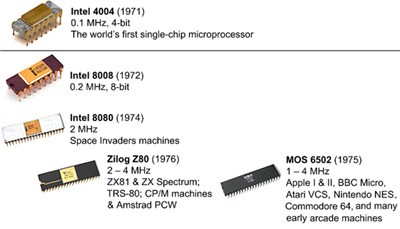
Things have come a long way since the Intel 4004, the first microprocessor was used. The Intel 8086 family of processors (known as x86) was so successful that a number of other chip manufacturers made their own versions of these chips. Companies like Cyrix, AMD and IBM produced 286, 386 and 486 processor clones. To counter this Intel trademarked the next generation chip with the name Pentium: competitors chose different names (K5, 5×86, etc). We will list each CPU as they evolved.
386 & 486
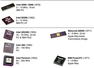
The 386 processor introduced wider 32-bit internal registers and a wide range of new instructions to take advantage of them. The 386 also included memory management circuits. The 486 improved on this.
Pentium
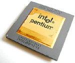
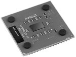
The original Pentium was essentially two 486 processors in one chip and contained 16KB of L1 cache (one 8KB cache for instructions or code, and another for data). It came in a 273-pin Pin Grid Array (PGA) package (known as Socket 4) and operated at 60 MHz. It was powered at 5V and generated enough heat to require a CPU cooling fan. The second generation Pentium came in a 296-pin Staggered Pin Grid Array (SPGA) package (Socket 7) in speeds from 75 to 166 MHz. The power-supply voltage level dropped to 3.3V, consuming less power and provide faster operating speeds. This design used an internal clock multiplier, which meant that the inside of the chip ran much faster than the main data bus that was attached to the processor. (This bus is called the Front-Side Bus or FSB). The Pentium also introduced a 64-bit external data bus. The internal design remained 32-bit, but the double-width interface allowed the CPU to move data in and out more quickly. The main competitors to the Pentium were the AMD K5 and Cyrix 5×86, and they were designed to use Socket 7. The AMD processor was designed in such a way that more processing was done in each clock cycle: in other words an AMD chip running at 100 MHz might perform as well as an Intel Pentium at 133 MHz. To solve this confusion, AMD chips were rated by the equivalent P-speed (e.g. P133 = equivalent to Pentium 133).
Pentium MMX
The third generation Pentium also used the 296-pin SPGA arrangement (Super Socket 7) and was produced in 166 – 233MHz speeds with 32KB cache. These devices had 57 extra instruction codes for multimedia work and were known as Pentium MMX processors. The K6 and MII are, respectively, the AMD and Cyrix equivalents of the MMX processor.
Pentium Pro
The Pentium Pro was designed for multi-processor systems. It used a 387-pin PGA (Socket 8) package; came with 16KB L1 cache and an onboard 256 or 512KB L2 cache
Pentium II / III class
Pentium II
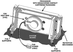
It used a new Single-Edge Contact (SEC) cartridge (also known as SECC). The 242-contact design is called Slot 1 and requires a special Fan Heat Sink (FHS) module and fan. The cartridge contains the Pentium II processor core (incorporating 32KB L1 cache) and 512KB L2 cache.
The K6-2 was AMD’s answer to the Pentium II and it added 21 further instructions to support multimedia work. It still used Super Socket 7.
Pentium III & Celeron
The original Pentium III was a Pentium II core with 512KB L2 cache. Speed increased to 600MHz, including a 100MHz front-side bus (FSB). Early models used Slot 1 but later version switched to the FC-PGA Socket 418 package. The Celeron was designed as a cheap version of the Pentium II & III. Originally the main difference was a lack of cache memory but later Celerons added cache. The chips originally came in Slot 1 designed but soon switched to Plastic PGA (PPGA) Intel Socket 370 packages.
AMD Athlon & Duron
The K7 Athlon originally ran at 500 MHz with 128KB L1 cache and a 512KB L2 cache. Early Athlon used Slot A, (mechanically identical to Slot 1 but different electrical connections), however, they soon switched to using Socket A. Duron was introduced as a cheap alternative, mimicking the Celeron. It also uses Socket A.
Pentium Xeon
The Xeon is the replacement for the Pentium Pro range: essentially a special version of the Pentium II for multiprocessor systems. They also featured up to 2MB of internal cache memory. Up to 32 Xeon processors could be mounted in a single system.
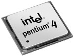
Pentium 4 class
Pentium 4
The early Pentium 4 used 423-pin PGA (Socket 423) but later models employed the improved Socket 478 package. The 64-bit external data bus of the Pentium design expanded to 128 bits and the minimum FSB speed increased to 400MHz. The core voltage dropped to 1.7V, allowing even faster execution — but the design requires a separate 12V power supply to the motherboard.
Athlon XP & Sempron
The Athlon XP range covers 1500 to 3000 (note that numbers are not MHz but Pentium speed equivalents). The Duron and lower-end Athlon XPs were renamed Sempron.
Pentium 4 HT (“Prescott”)
Hyper threading is Intel’s name for a design that duplicates many parts of the processor, allowing two program threads to run simultaneously, but not as quickly as a full dual core.
Xeon & Athlon MP
The (P4-based) Xeon and Athlon MP processors are designed for multiprocessor systems.
Pentium M
The Pentium M is a variant of the Pentium 4 designed specially for laptops. It significantly outperforms the P4 at the same clock speed. The Pentium M forms part of the Intel Centrino chipset, along with wireless networking support chips.
The shift to 64-bit
Itanium & Itanium 2
The Itanium was a drastic departure from the x 86 designs. A new, more efficient 64-bit instruction set was introduced (known as IA-64) but this was totally incompatible with i386 programs. Hence the processor did not catch on, and is only used in high-end server systems. The Itanium is mounted in a Pin Array Cartridge (PAC).
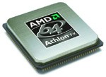
AMD Athlon 64 & Sempron/64
The Athlon 64 also featured a new 64-bit instruction set but it maintained full compatibility with the older i386 codes. This design is called AMD64, x86-64 or more commonly x64. The Athlon 64 introduces a new processor socket: Socket 754, which looks similar to the newer Pentium 4 Socket 478 and Xeon Socket 603 and uses the same type of mPGA connectors. As with the Pentium 4 processor, motherboards for the Athlon 64 also require the ATX12V connector to provide adequate 12V power. The Sempron/64 is intended to cover the lower end of the Athlon market and fits in socket 754.
Pentium 4 EM64T, Celeron D
Intel knew they were in trouble when the Athlon 64 appeared. Therefore they introduced versions of the P4 and Celeron that support the x86-64 instruction set. However, they refer to these instructions as EM64T codes. Note that Celeron D does not contain dual cores.
Athlon64 X2, Pentium D & Pentium M Dual Core
These feature dual cores: multiprocessor systems can be expensive but an alternative is to mount two processor cores in the same package, sharing some circuitry.
Xeon EM64T & AMD Opteron
The Xeon EM64T supports the x86-64 instruction set.
The Opteron is AMD’s equivalent to the Xeon EM64T and is aimed at the server market.
AMD Turion 64
The Turion 64 is designed to compete with the Pentium M in the laptop market. This uses the new Socket S.
Last of the 32-bit processors
Intel Core Duo
The 32-bit processor market is not dead. In January 2006 Intel announced the Core Duo processors that would be used in laptops (branded as part of the Centrino Duo chipset) and also the new range of Apple iMacs. The Core Duo replaces the Pentium M and significantly outperforms it at the same clock frequency. Core Solo is a scaled-down version with only one core.
The CPU socket information is summarized in this table
| Processor | Clock Rate (in GHz) | Socket | Core Count | Bus Speed (MHz) | L2 Cache | L3 Cache (MB) |
| Intel Atom | Upto 2 | PBGA437 | 1,2 | 400-667 | 512 KB – 1 MB | – |
| Intel Pentium Dual-Core | 1.33- 2.93 | 775,M,P,T | 1,2 | 533-1066 | 1 MB – 2 MB | – |
| Intel Core 2 Duo | 1.06- 3.33 | 775,M,PT | 1,2,4 | 533-1600 | 1 MB – 12 MB | – |
| Intel Core i3 | 2.4- 3.06 | LGA 1156 | 2 | 1066-1600 | 256 KB | 3 – 4 |
| Intel Core i5 | 1.06- 3.46 | LGA 1156 | 2,4 | 2.5 GigaTransfer/s | 256 KB | 4 – 8 |
| Intel Core i7 | 1.6- 3.33 | LGA 1156 | 4,6 | 4.8-6.4 GT/s | 4/6 ×256 KB | 6 – 12 |
| Opteron | 1.7-2.5 | AM2 | 4 | 1000 | 256, 512 KB | 2 |
| Phenom | 1.9-2.4 | AM2+ | 3 | 1600-1800 | 512 KB | 2 |
| Phenom II | 2.6-3.4 | AM2+ , AM3 | 4, 6 | 1800-2000 | 512 KB | 6 |
| Athlon | 2.4-2.7 | AM2+ | 1 | 1600- 1800 | 512, 1024 KB | |
| Athlon II | 2.2-3 | AM2+ | 2 , 4 | 1600-2000 | 512-1024 KB | |
| Sempron | 2.7 | AM2+ | 1 | 1600 | 512 KB |
Apply for IT Support Certification
https://www.vskills.in/certification/certified-it-support-professional
